Overview of the Plasma Coating Process

Benjamin Lawrence | March 26, 2021
Nanocoatings, thin films measured at the nanolevel, serve numerous purposes. But for many product design engineers, the ability to safeguard electronics with protection capabilities such as hydrophobicity, corrosion-resistance, and dielectric and thermal properties, is top of the list. Protective nanocoatings empower organizations to mitigate risk associated with downtime, reduce repairs and warranty claims, and cultivate market confidence with remarkably reliable electronic products.
Read our white paper on thin-film coating deposition methodologies, including PECVD
Plasma Surface Technology Benefits
Plasma application processes can produce nanocoatings with many beneficial substrate surface characteristics, including:
- Hydrophobicity
- Oleophobicity
- Humidity/temperature protection
- Excellent flammability protection
- Low dielectric constant with good high-frequency properties
- Good dielectric strength and high bulk and surface resistance
- Splash protection
- High barrier protection against corrosive chemicals and gases while providing low permeability to moisture
These valuable benefits have piqued interest in plasma-based nanocoatings and the processes used for their deposition.
Plasma Coating Processes
While several methodologies exist to apply nanocoatings to substrates, including plasma spray deposition, plasma-enhanced chemical vapor deposition (PECVD) is a popular method due to enhanced process control and beneficial physical film properties.

PECVD Process
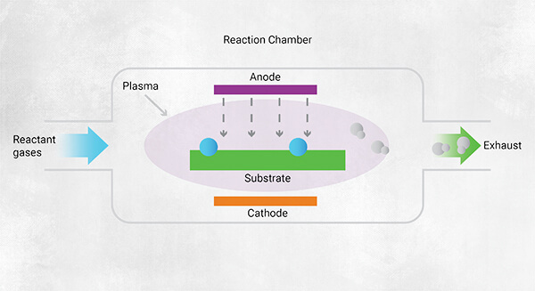
The PECVD Plasma Application Process
PECVD harnesses plasma energy to deposit nanocoatings through several power sources, including microwave discharge, radiofrequency, and direct current. Using PECVD equipment, gases are energized to form a plasma and a mixture of ions, radicals, excited atoms, free electrons, and molecules to deposit the nanocoatings.
Possible materials to form the coatings include metals, polymers (silicones, hydrocarbons, fluorocarbons), oxides, and nitrides, representing a wide range of possibilities. The resulting films are highly cross-linked, dense, pinhole-free, and uniform; these attributes lend to good physical properties.
The process offers precision control over these film properties, yielding various chemical, thermal, mechanical, electrical, and optical benefits.

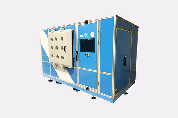
HZO PRO800-PL Proprietary Nanocoating Equipment
PECVD Parameters to Consider for Optimal Performance
Internal and external plasma parameters may be modified to affect the resulting film. Internal plasma parameters include the precursors used, distribution of various species in the plasma and the species’ energy, and homogeneity of discharge. External parameters include temperature, applied power, total pressure, gas flow rates, pumping speed, and reactor geometry.
PECVD Benefits
The deposition process allows for a wide range of material usage, including unconventional precursors that can deposit on surfaces with complex geometries, typically at lower temperatures than other vacuum deposition processes such as thermal chemical vapor deposition. It is possible to tightly and efficiently control these precursors while generating few by-products, allowing for precise control of film composition and uniformity. As a result, PECVD nanocoating chemistry is unique and often unobtainable with standard liquid coating deposition methods.
Possible materials to form the coatings include metals, polymers (silicones, hydrocarbons, fluorocarbons), oxides, and nitrides, representing a wide range of possibilities.
PECVD Applications
PECVD coatings are used in applications that require lower cost and high efficiency, including optical coatings, corrosion resistance, and dielectric films.
Applications include:
- Mobile phones
- Earbuds
- Smart speakers
- Wearables
- Outdoor cameras
- Hearing aids
- Catheters
- Smart patch
- Connected health devices
- Automotive in-cabin sensors and electronics
- Automotive cabin filters
- Automotive cameras
- Doorbell cameras
- POS scanners
- Air quality sensors
- Smart home applications
- LEDs
- Drones
- HVAC sensors
- Industrial equipment controller
PECVD Coatings with HZO
At HZO, our in-house designed deposition equipment is optimized for faster deposition rates with reactors that are scalable for High-Volume Manufacturing (HVM). The fixtures used during the deposition process (directional plasma only) provide an alternative to masking, a process used to ensure coating does not cover parts such as connectors. This alternative can save time and money, as masking and demasking can be labor-intensive.
- Plasma-based technology leverages a variety of chemistries that can quickly be adapted to specific requirements.
- Coatings can be single or multi-layer, with one or more chemistries being applied. This hybrid approach allows the delivery of target properties.
- Materials include halogen-free alternatives.
- Typical thickness varies from 300 nm to 3 µm.
- Masking requirements can generally be addressed in the chamber as part of the deposition process using a shadow mask to isolate areas to be kept free of coating.
- Minimal footprint required to perform coating operation.
- Features include liquid protection, anti-corrosion, etc.
- Solutions are scalable for high volume manufacturing at competitive pricing
Download the HZO Sentinel Series™ Datasheet
For more information on our plasma-based nanocoatings, feel free to reach out to the HZO team here with any questions or concerns. Our engineers would love to give you a free consultation to determine if the plasma nanocoating process is ideal for your application.
At HZO, our in-house designed deposition equipment is optimized for faster deposition rates with reactors that are scalable for High-Volume Manufacturing (HVM).
Benjamin Lawrence
Benjamin is an experienced and enthusiastic engineering consultant with experience in PECVD, thermal CVD, ALD, research, design, operations, mass production, and process development.

Discover how HZO can protect your product
